Advanced Hardware and PCB Design Masterclass 2022 -EsteemPCB
Loại khoá học: Engineering
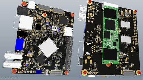
Advanced Hardware Design Course Part-1 RK3399 COB (LPDDR4 SDRAM, WIFI/BT, EMMC, PMIC, 260 Pin DDR4 System on Module)
Mô tả
I have Divided this Course into #13 Different Sections Under Each Section You will find Multiple Lessons:
Section 1: Discuss the Requirement sheet and Processor RK3399 Datasheet in very detail.
Section 2: How to Choose an SDRAM (SDR/DDRX/LPDDRX) ? from Very Scratch and Its Pin Mapping and Schematic Design From Datasheet.
Section 3: Selection and Schematic Design of PMIC (Power Management IC) in very Details.
Section 4: EMMC (Embedded Multimedia Card) Chip Selection, Pin Mapping, and Schematic Design.
Section 5: WIFI/BT Module Selection, Certification (US/EU/CA), Selection, and Schematic Design.
Section 6: Selection of External LDO/DC-DC/Buck-Boost and Their Schematic Design in very Details.
Section 7: Schematic Design of RK3399, Pin Mapping and Impedances Planning on Schematic through Net-Classes.
Section 8: Layer Stack up(4/6/8/12L), Finish the Components Placement Planning and its Execution Part-1
Section 9: Components Placement Planning and its Execution Part-2
Section 10: Components Placement Planning and its Execution Part-3
Section 11: Layout Planning, Preliminary Layout, High-Speed Design Rules and Length Matching, Power Plane Planning by Sections, Optimization of Layout Part-1
Section 12, 13: Power Plane Planning by Sections, Optimization of Layout.
Major Schematic Blocks that I have designed in this course are Project Block Diagram, "Power Budget Block Diagram", "Power Supply Schematic for RK3399", "PMUIO Schematic Block of RK3399", "EMMC/PCIe/ADC Schematic for RK3399", "EDP/MIPI-DSI/HDMI Schematic for RK3399", "Type-C/USB3.0/USB2.0 Hosts Schematic for RK3399", "MIPI-CSI/GPIOs/I2C Schematic of RK3399", "MII/RMII/GMII/RGMII Schematic for RK3399", "SDR/DDRx/LPDDRx Schematic For RK3399", "PMIC/DC-DC/LDOs/Buck-Boost for RK3399" and many more various subparts you will learn in this course as you can see on the curriculum sections and their lessons.
You will also learn some basic hardware designing blocks as well as You will also learn some Basic Blocks as well:
Pre-Schematic Design Blocks (Block Diagram and Power Budget)
Layer Stack-up Selection and Rules for Defining any Stack-up
Different Grounding Techniques( Signal Grounding, Earth Grounding, Chassis Grounding)
Power Distribution Network Analysis (PDN Analysis) of any PCB.
and many more things.
Ferrite Bead, ESD Diodes, and Magnetic Application and their selection.
How to do Placement and Layout Planning on Microsoft-Paint and many more.
After the completion of this course, you can design any "Processor Board" without any Simulation models and third-party support.
Bạn sẽ học được gì
How to Extract Selection information from Requirement Sheet for Processor, SDRAMs, EMMC, WIFI/BT modules etc.
How to Choose a Processor by Defining its No. of Core, Cache, Bandwidth, Clock requirements.
Different Architecture of Processor for Ex. Little-big, and Memory Organization.
Types of Internal and External SDRAMs (DDRX, LPDDRX, and their Enhanced versions).
Comparisons of External SDRAMs up-to DDR5 and LPDDR5
Different Signal Groups of SDRAM (Data, Address & command, Control and Clock Groups)
Develop a Set Procedure on selection of SDRAM, PMIC, EMMC, WIFI Module, Processor for Mobile Application.
How to Read the Datasheet of Different components used in this Board RK3399, 2GB LPDDR4 SDRAM, 16GB EMMC, PMIC, WIFI/BT Module etc.
Pin Mapping of SDRAM, EMMC, SDIOs, MIPIs, EDPs, Type-C, USB3.0 & 2.0, SDMMC etc. with RK3399 on a Simple Excel Sheet.
How to Design the Schematic of Processor, SDRAM, EMMC, WIFI, PMIC using their Respective datasheets and Design Guidelines Documents.
Discussion of Different WIFI/BT Module Certification and Regulation as per US, Europe, Canada etc.
Impedance Profile Planning of More than 1000 interconnects on a Excel Sheet.
Layer Stack up (4/6/8/12L), Finish the Components Placement Planning and its Execution.
Layout Planning, Preliminary Layout, High Speed Design Rules and Length Matching, Power Plane Planning by Sections, Optimization of Layout Loop-1 and Loop-2
FAN-OUT of #828 Balls of RK3399, #200 Balls of LPDDR4 SDRAM and #180 Balls of EMMC.
Yêu cầu
- Student should have Understanding of Board Design.
- Student should have Completed the Complex Mixed Signal Board Design Course.
- Student should have Patience and Determination to complete the course which has more than 10,000 interconnects and Lot of Dense Components to route.
- For this course Student should have "Altium Designer" Installed on their PC / Laptop
- You do not need any prior knowledge of "Altium Designer" because we'll going to do everything from scratch.
Nội dung khoá học
Viết Bình Luận
Khoá học liên quan


Đăng ký get khoá học Udemy - Unica - Gitiho giá chỉ 50k!
Get khoá học giá rẻ ngay trước khi bị fix.
Đánh giá của học viên
Bình luận khách hàng