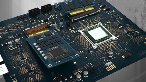
PCB Design using OrCAD/Allegro from Basics to Expert level
Loại khoá học: Hardware
Learn OrCAD/Allegro PCB Design: Schematic (OrCAD Capture), Footprint's (Package Editor) & Board Design(PCB Editor)
Mô tả
PCB Design and electronics circuits are basements for all type of electronics products. PCBs are derived from the analog and digital circuits which are prepared according to the application required. Printed circuit boards are the main pillars of the Electronics world. Every Electronics products has PCB inside it, from consumer gadgets like computers, smart phones and gaming consoles to industry and even high-tech products.
"Welcome to our comprehensive online PCB Design course, a journey that will take you from the basics to an expert level in PCB design using the powerful Cadence suite of tools - OrCAD and Allegro. This course is designed to equip you with the knowledge and skills needed to create professional-grade Printed Circuit Boards (PCBs).
Why Choose Our PCB Design Course?
Our course is the ultimate choice for individuals who are passionate about PCB design or wish to establish a career in this field. Here's what sets us apart:
In-Depth PCB Design Knowledge: We provide a deep and thorough understanding of PCB design principles, covering everything from the fundamental concepts to advanced techniques.
Comprehensive Tool Training: Gain mastery over the industry-standard OrCAD and Allegro tools by Cadence. Learn how to create schematics using OrCAD Capture, design footprints with Package Editor, and craft intricate board layouts with PCB Editor.
Online Education, Your Way: Experience the convenience of online learning. Our course is designed to be flexible, allowing you to learn at your own pace, at any time and from anywhere in the world.
Best-in-Class Instruction: Learn from experienced instructors with extensive expertise in PCB design. Benefit from their real-world industry insights and best practices.
Practical Projects: Apply your newly acquired knowledge to real-world projects, ensuring you develop the practical skills needed to excel in the industry.
Course Highlights:
PCB Design Fundamentals: Start with the basics of PCB design, including understanding components, schematics, and layout principles.
OrCAD Overview: Dive into OrCAD's capabilities through OrCAD Capture, and learn to create comprehensive schematics for your PCB projects.
Allegro Mastery: Transition to Allegro, delving into advanced features for complex PCB layouts, and create footprints with ease using Package Editor.
Professional-Grade Design: Progress to creating intricate PCB layouts with precision, while learning how to troubleshoot and optimize your designs for peak performance.
Hands-On Practice: Our course includes practical projects and exercises that reinforce your learning. This practical experience ensures you can confidently tackle real-world PCB design challenges.
Expert Guidance: Access guidance and support from our experienced instructors who are dedicated to your success.
Why PCB Design Matters:
PCB design is at the heart of the modern electronics industry. As technology advances, the demand for skilled PCB designers who can create efficient and compact circuit boards continues to grow. This course will empower you to meet this demand.
Start Your Journey Today:
Join us on your path to becoming a PCB design expert. This course equips you with the knowledge, tools, and hands-on experience to stand out in the field. Whether you aspire to work for top electronics companies, launch your PCB design business, or embark on a personal project, this course is your essential stepping stone.
Enroll Now:
Don't miss the opportunity to access the best PCB design education available online. Enroll now and take the first step toward mastering PCB design with OrCAD, Allegro, and Cadence. Your path to expertise in PCB design begins here!"
Required eligibility:
Diploma in Electrical or Electronics & Communication.
BE/BTech. in Electrical or Electronics & Communication.
BSc/MSc in Electronics & Communication.
ME/MTech. (E&CE) in Communication.
PCB Design Course Content is given below in brief:
Schematic Design:
Basic Electronics theory.
Basics of Circuit designing.
Schematic design preparation.
Schematic part editing and creation.
Net list and Net class creation.
Bill Of Material generation (BOM).
Electrical Rule Checking.
Footprint Creation:
Through hole footprint creation.
Surface Mount Device footprint creation.
BGA/PGA footprint creation.
Board Designing:
Board size and shape creation.
Component placements.
PCB Routing.
Plane creation.
Design rule checking.
Gerber generation.
Skills you gain after the course completion:
Basic Electronics and Electronic components expertise.
Circuit Designing (Power management circuit designing)
Circuit Simulation for best understanding of the subject.
Tools/Software Expertise.
Basic design module practice up to 2-Layers.
Advanced design module practice up to 6-Layers.
Design expertise:
Assignments consists single and double sided PCB.
Assignments consists 2-Layers, 4-Layers and 6-Layers design.
Library Module:
Symbol and Footprint design for all types of packages.
Normal Placements & critical placement techniques
Normal Routing and Critical Routing techniques.
Gerber Creation.
Benefits of choosing PCB Design Course:
Strong hold in basic electronics.
Circuit Design capability.
Circuit analysis & ERC.
Components knowledge.
Power Supply designing.
PCB-CAD tool expertise.
Expert in library creation.
Multi-layer PCB designing.
Gerber Creation.
Bạn sẽ học được gì
You will learn Basic Electronics Theory, Circuit Design and Analysis, Basics of Printed Circuit Board, Electronic Components and Instruments. Study notes given.
You will work on Printed Circuit Board Layout Design such as Schematic creation, Library Creation: Electronic Symbol and Package (Footprint Creation) Designing.
Switching schematic to Board Design (Netlist Creation), Thorough knowledge on Constraint Management Settings, Board Shape Creation (DXF import included) & DRC.
Work on Single sided Board Design, Double sided Board Design, Via creation and application. Routing on Top and Bottom Layer includes enough practice modules.
Plan Creation of Power and Ground. Also Split Plan Creation. Design Rule Checking and DRC updates. Work on Artwork. Setting up all required film layer setups.
Gerber Generation and Gerber analysis and improvements. PCB Manufacturing overview. Latest topics will be updated on regular basis and will be informed about it
Yêu cầu
- Basic Electronics knowledge, BSc(Electronics), Diploma (Electronics or Electrical), BE (Electronics or Electrical), Master degree in Electronics and Electrical
- If you are working in PCB Manufacturing and Assembly unit, PCB Design course will be an added skillset to your career profile.
- If you own PCB printing, assembly and component soldering unit, you can learn PCB Design and can extend your business unit towards service sector.
- If you have passion on Electronics subject, you can enroll this course and convert your passion into career.
Nội dung khoá học
Viết Bình Luận
Khoá học liên quan


Đăng ký get khoá học Udemy - Unica - Gitiho giá chỉ 50k!
Get khoá học giá rẻ ngay trước khi bị fix.
Đánh giá của học viên
Bình luận khách hàng