High-Speed Board Design Course System On Module -EsteemPCB
Loại khoá học: Engineering
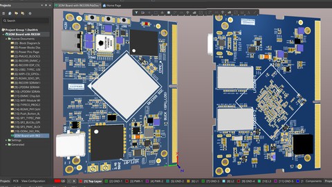
Advanced Hardware Design Course of SOM (RK3399, LPDDR4 SDRAM, WIFI/BT Module, EMMC, PMIC, 260 Pin DDR4 System on Module)
Mô tả
I have Divided this Course into #13 Different Sections Under Each Section You will find Multiple Lessons:
Section 1: Discuss the Requirement sheet and Processor RK3399 Datasheet in very detail.
Section 2: How to Choose a SDRAM (SDR/DDRX/LPDDRX) ? from Very Scratch and Its Pin Mapping and Schematic Design From Datasheet.
Section 3: Selection and Schematic Design of PMIC (Power Management IC) in very Details.
Section 4: EMMC (Embedded Multimedia Card) Chip Selection, Pin Mapping and Schematic Design.
Section 5: WIFI/BT Module Selection, Certification (US/EU/CA), Selection and Schematic Design.
Section 6: Selection of External LDO/DC-DC/Buck-Boost and Their Schematic Design in very Details.
Section 7: Schematic Design of RK3399, Pin Mapping and Impedances Planning on Schematic through Net-Classes.
Section 8: Layer Stack up(4/6/8/12L), Finish the Components Placement Planning and its Execution Part-1
Section 9: Components Placement Planning and its Execution Part-2
Section 10: Components Placement Planning and its Execution Part-3
Section 11: Layout Planning, Preliminary Layout, High Speed Design Rules and Length Matching, Power Plane Planning by Sections, Optimization of Layout Part-1
Section 12, 13: Power Plane Planning by Sections, Optimization of Layout.
Major Schematic Blocks that I have designed in this course are Project Block Diagram, "Power Budget Block Diagram", "Power Supply Schematic for RK3399", "PMUIO Schematic Block of RK3399", "EMMC/PCIE/ADC Schematic for RK3399", "EDP/MIPI-DSI/HDMI Schematic for RK3399", "Type-C/USB3.0/USB2.0 Hosts Schematic for RK3399", "MIPI-CSI/GPIOs/I2C Schematic of RK3399", "MII/RMII/GMII/RGMII Schematic for RK3399", "SDR/DDRx/LPDDRx Schematic For RK3399", "PMIC/DC-DC/LDOs/Buck-Boost for RK3399" and many more various subparts you will learn in this course as you can see on the curriculum sections and their lessons.
You will also Learn some basic hardware designing blocks as well like You will also learn some Basic Blocks as well:
Pre-Schematic Design Blocks (Block Diagram and Power Budget)
Layer Stack-up Selection and Rules for Defining any Stack-up
Different Grounding Techniques( Signal Grounding, Earth Grounding, Chassis Grounding)
Power Distribution Network Analysis (PDN Analysis) of any PCB.
and many more things.
Ferrite Bead, ESD Diodes, and Magnetic Application and their selection.
How to do Placement and Layout Planning on Microsoft-Paint and many more.
After the completion of this course you can design any "Processor Board" without any Simulation models and third party support.
Bạn sẽ học được gì
Yêu cầu
Nội dung khoá học
Viết Bình Luận
Khoá học liên quan


Đăng ký get khoá học Udemy - Unica - Gitiho giá chỉ 50k!
Get khoá học giá rẻ ngay trước khi bị fix.
Đánh giá của học viên
Bình luận khách hàng